GaNdalf II CoolGaN-Based Digital Power Factor Correction Development System
New, improved Future Electronics blueprint for bridgeless PFC circuit design
- >99% peak efficiency
- Latest GaN power components
- Low component count
- Adaptable and flexible development platform
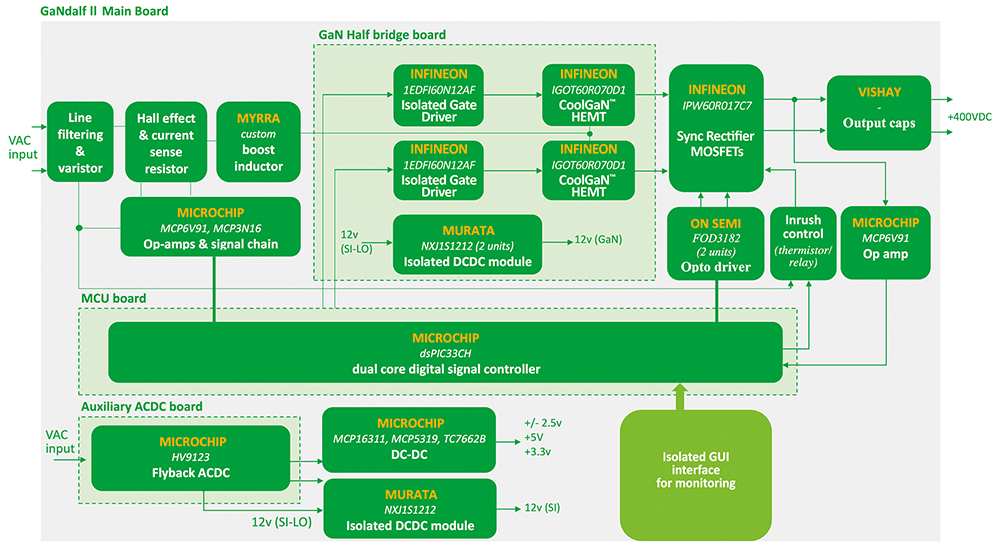
The new GaNdalf II development system features components from leading suppliers of technology supporting the bridgeless totem-pole Power Factor Correction (PFC) topology, including:
- Infineon – CoolGaN™ enhancement mode gallium nitride (GaN) transistors. These devices provide higher efficiency because of the superior electrical properties of the wide-bandgap GaN material. CoolGaN transistors provide better switching performance and lower switching losses than equivalent silicon-based MOSFETs.
- Microchip – dual-core 16-bit Digital Signal Controller (DSC)
Offering a peak efficiency of >99% and Total Harmonic Distortion (THD) of <5%, GaNdalf II is the ideal starting point for highly efficient power conversion designs supplying loads up to 2kW.
GaN Power Switch: The Crucial Technology Enabling the Ultra-Efficient Bridgeless Totem Pole Topology
Power Factor Correction (PFC) is widely used in AC-DC power supplies with an input power greater than 75W. The PFC circuit controls the input current to synchronize it with the input voltage and to minimize reactive power losses.
Power-system designers are under more pressure than ever to achieve high efficiency across the whole AC-DC converter circuit. In the PFC stage, the drive for efficiency has led designers to evaluate various bridgeless PFC circuit topologies, which remove the rectifying diode bridge and its associated power losses from the input of the PFC stage.
The bridgeless totem pole PFC topology offers various advantages compared to other approaches, including:
- Fewer components
- Lowest conduction losses
- Highest efficiency
Conventional silicon super-junction MOSFETs are unsuitable for use in the hard-switched half-bridge arrangement in a bridgeless totem-pole topology, which calls instead for the superior characteristics – including low output capacitance and zero reverse recovery – of GaN High Electron-Mobility Transistor (HEMT) switches.
In the GaNdalf II system, CoolGaN™ devices from Infineon offer outstanding performance when operating in continuous conduction mode, helping the PFC stage to achieve efficiency of 99.0%.

GaNdalf II is supplied to pre-qualified customers of Future Electronics. For more information, contact your local branch.


GaNdalf II
Key Components of the GaNdalf II Power System
|
Key Features of the GaNdalf II PFC Circuit
|


