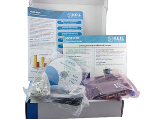
Référence fabricant
LPC1768FBD100,551
IC MCU 32BIT 512KB FLASH 100LQFP
NXP LPC1768FBD100,551 - Spécifications du produit
Informations de livraison:
ECCN:
Informations PCN:
Statut du produit:
NXP LPC1768FBD100,551 - Caractéristiques techniques
| Family Name: | LPC17xx |
| Core Processor: | ARM Cortex M3 |
| Program Memory Type: | Flash |
| Flash Size (Bytes): | 512kB |
| RAM Size: | 64kB |
| Speed: | 100MHz |
| No of I/O Lines: | 70 |
| InterfaceType / Connectivity: | CAN/Ethernet/I2C/I2S/SPI/SSP/UART/USB |
| Peripherals: | CAN/Ethernet/I2C/I2S/On-Chip-ADC/PWM/SPI/SSP/UART/USB/Watchdog |
| Number Of Timers: | 4 |
| Supply Voltage: | 2.4V to 3.6V |
| Operating Temperature: | -40°C to +85°C |
| On-Chip ADC: | 8-chx12-bit |
| Watchdog Timers: | 1 |
| Style d'emballage : | LQFP-100 |
| Méthode de montage : | Surface Mount |
Fonctionnalités et applications
The LPC1768FBD100 are ARM Cortex-M3 based microcontrollers for embedded applications featuring a high level of integration and low power consumption. The ARM Cortex-M3 is a next generation core that offers system enhancements such as enhanced debug features and a higher level of support block integration.
The LPC1768 operate at CPU frequencies of up to 100 MHz. The LPC1769 operates at CPU frequencies of up to 120 MHz. The ARM Cortex-M3 CPU incorporates a 3-stage pipeline and uses a Harvard architecture with separate local instruction and data buses as well as a third bus for peripherals. The ARM Cortex-M3 CPU also includes an internal prefetch unit that supports speculative branching.
Features :
- ARM Cortex-M3 processor, running at frequencies of up to 100 MHz (LPC1768/67/66/65/64/63) or of up to 120 MHz (LPC1769). A Memory Protection Unit (MPU) supporting eight regions is included.
- ARM Cortex-M3 built-in Nested Vectored Interrupt Controller (NVIC).
- Up to 512 kB on-chip flash programming memory. Enhanced flash memory accelerator enables high-speed 120 MHz operation with zero wait states.
- In-System Programming (ISP) and In-Application Programming (IAP) via on-chip bootloader software.
- On-chip SRAM includes
- 32/16 kB of SRAM on the CPU with local code/data bus for high-performance CPU access.
- Two/one 16 kB SRAM blocks with separate access paths for higher throughput. These SRAM blocks may be used for Ethernet, USB, and DMA memory, as well as for general purpose CPU instruction and data storage.
- Four reduced power modes: Sleep, Deep-sleep, Power-down, and Deep power-down.
- Single 3.3 V power supply (2.4 V to 3.6 V).
- Four external interrupt inputs configurable as edge/level sensitive. All pins on Port 0 and Port 2 can be used as edge sensitive interrupt sources.
- Non-maskable Interrupt (NMI) input.
- Clock output function that can reflect the main oscillator clock, IRC clock, RTC clock, CPU clock, and the USB clock.
- The Wake-up Interrupt Controller (WIC) allows the CPU to automatically wake up from any priority interrupt that can occur while the clocks are stopped in deep sleep, Power-down, and Deep power-down modes.
- Crystal oscillator with an operating range of 1 MHz to 25 MHz.
- 4 MHz internal RC oscillator trimmed to 1 % accuracy that can optionally be used as a system clock.
- USB PLL for added flexibility.
- Code Read Protection (CRP) with different security levels.
- Unique device serial number for identification purposes.
- Available as 100-pin LQFP package (14 mm × 14 mm × 1.4 mm).
To learn more about LPC1768x product family, Click Here
Emballages disponibles
Qté d'emballage(s) :
90 par Tray
Style d'emballage :
LQFP-100
Méthode de montage :
Surface Mount


