
Infineon 1200 V CoolSiC™ MOSFET Generation 2
Significant improvements over Generation 1 in key figures of merit for both hard- and soft-switching topologies
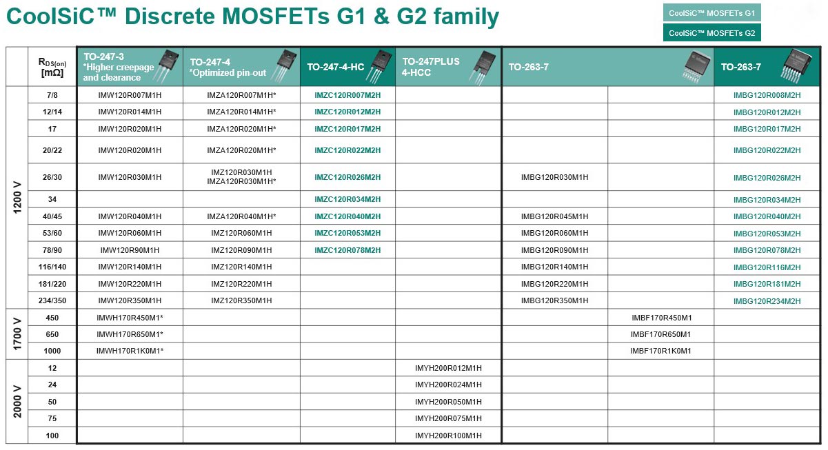
Infineon's 1200 V silicon carbide (SiC) CoolSiC MOSFETs are built on a state-of-the-art trench semiconductor process optimized to allow for both the lowest losses in an application and the highest reliability in operation. This whole discrete CoolSiC MOSFET portfolio comes in 650 V, 750 V, 1200 V, 1700 V, and 2000 V voltage classes, with on-resistance ratings from 7 mΩ up to 1000 mΩ.
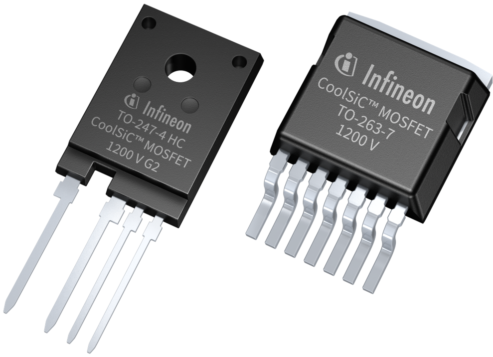
Devices in the TO-274-4 package have been added to the CoolSiC G2 portfolio with increased creepage distance, thin signal leads and Kelvin pins to prevent solder bridging, and optimized thermal interface material (TIM) area for superior thermal performance. The standard TO-247-4 package allows for pin compatibility with the majority of offerings in the market. Other CoolSiC 1200 V Generation 2 devices are offered in the D²PAK-7L (TO-263-7) package.
CoolSiC™
CoolSiC trench technology enables a flexible parameter set to implement application-specific features in respective product portfolios, e.g., gate-source voltages, avalanche specification, short-circuit capability, or internal body diode rated for hard commutation.
Reference Design
The REF-DR3KIMBGSIC2MA SiC reference design consists of two PCBs, including a driver circuit and a 3-phase inverter for servo motors and drives. Benefits include high power density, passive cooling without cooling fans, and an ultra-small footprint with a PCB diameter of only 110 mm.
Comparison of CoolSiC G2 to G1
|
|

Features and Benefits
| Applications
|

