
onsemi NCP51100A Single 2 A High-Speed, Low-Side Gate Driver
The onsemi NCP51100 2 A gate driver is designed to drive an N channel enhancement-mode MOSFET in low-side switching applications by providing high peak current pulses during the short switching intervals. The driver is available with TTL input thresholds. Internal circuitry provides an under-voltage lockout function by holding the output LOW until the supply voltage is within the operating range.
The NCP51100 delivers fast MOSFET switching performance, which helps maximize efficiency in high frequency power converter designs. NCP51100 drivers incorporate MillerDrive™ architecture for the final output stage. This bipolar-MOSFET combination provides high peak current during the Miller plateau stage of the MOSFET turn-on / turn-off process to minimize switching loss, while providing rail-to-rail voltage swing and reverse current capability. The NCP51100 is available in industry standard, 5-pin, SOT23.
Features
| Applications
|
Benefits
| End Products
|
NCP51100 Internal Block Diagram

NCP51100 Typical Application

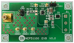
onsemi NCP51100 EVB Single 2A Low-Side Gate Driver Evaluation Board
This NCP51100 EVB is a proposed solution for the high speed dual gate driver using the NCP51100. This user kit also includes information regarding operating procedures, input/output connections, an electrical schematic, printed circuit board (PCB) layout, and a bill of material (BOM) for the evaluation board.
 NCP51100 EVB User's Manual | Key Features:
|