FTM / Security & Encryption / Future Electronics — Running Real-Time Applications on an FPGA SoC


By Patrice Brossard
EMEA Vertical Segment Manager (FPGAs and ASICs), Future Electronics
The inexorable progress of integration in semiconductors has been blurring the boundaries between different types of components for many years. By loading up one type of component with IP from a different kind, a sensor can become a machine learning inference engine, a microcontroller can be made to behave like an applications processor, or a non-volatile memory can provide a secure hardware root-of-trust.
Late in 2019, this blurring took another step forward with the merging of two types of system which have almost completely different sets of attributes: an FPGA, and processors running real-time applications in a Linux® operating environment. An FPGA is a programmable hardware fabric which supports the parallel processing of multiple concurrent tasks, while a processor is a hardware platform for executing a fixed instruction set architecture (ISA), and supports the serial processing of threads of instructions.
The 2019 introduction of the Microchip PolarFire® SoC FPGA bolted together these two component types, creating a single system-on-chip which provides:
This means that electronics system architects now have the option of using a single chip which offers both the low power consumption, high thermal efficiency and defense-grade security of an FPGA, and the deterministic execution capabilities provided by a fast processor.
This hybrid architecture clearly requires a system design engineering team to straddle the two worlds of the FPGA and the microprocessor. So what are the challenges involved in integrating these two types of hardware system into a single, reliable end product design? This hybrid SoC platform offers unique capabilities and advantages in applications such as systems operating in environments subject to extreme temperatures, artificial intelligence (AI) inferencing at the edge, security-conscious applications, aerospace and defense systems, and communications infrastructure. But is the difficulty of combining these two product types worth accepting to gain these advantages?
Understanding the hybrid processor/FPGA architecture
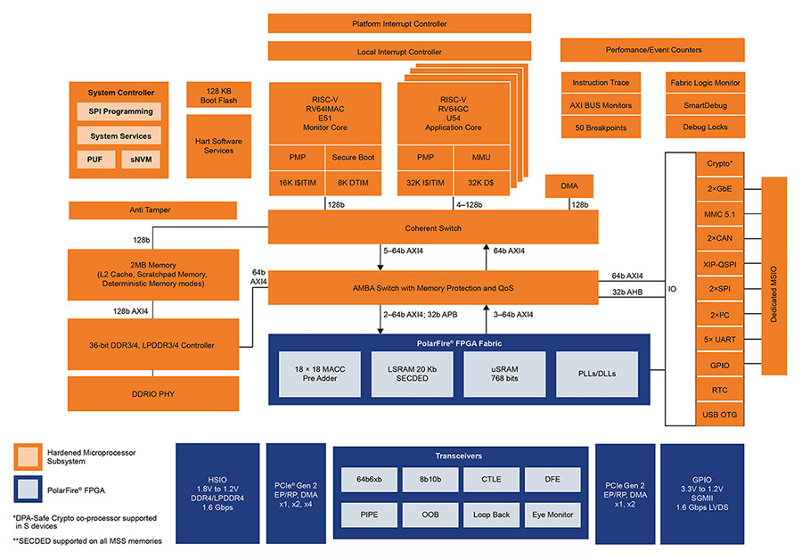
At the heart of the PolarFire SoC FPGA is a deterministic, coherent CPU cluster of 4+1 RISC-V cores, as shown in Figure 1. RISC-V is a free and open functional specification for a processor’s ISA, and is backed by a growing ecosystem of development professionals, specifications, software and other resources.
For the CPU cluster in the PolarFire SoC, Microchip has developed its own hardware architecture in collaboration with RISC-V specialist SiFive. A unique feature of the Microchip implementation is the freedom to turn off CPU branch prediction and make the memory sub-system fully deterministic.
This eliminates all variation in execution time while maintaining the high processor performance provided by the four RISC-V cores, and also making use of the deterministic features of the PolarFire FPGA.
The fifth core, a monitor core, is used to manage the boot process and system configuration. Unlike the application processing cores, it does not include virtual memory support.

Fig. 1: The PolarFire SoC architecture combines separate FPGA hardware and a CPU cluster. (Image credit: Microchip)
All the SoC’s memories feature ECC with single error detection, providing a very high level of data integrity, which is a mandatory requirement in safety-critical applications, for instance in aerospace systems.
A hallmark of the PolarFire SoC FPGA is its very low power consumption: Figure 2 shows a comparison of the PolarFire SoC’s power usage as a function of CoreMark® processor loading against that of traditional Arm® Cortex®-A microprocessor cores.

Fig. 2: Comparison of power consumption between the PolarFire SoC and Arm Cortex-A microprocessor cores. (Image credit: Microchip)
This is clearly advantageous in battery-powered systems, but not only there: in any system, low power consumption can eliminate the need for a heat-sink or fan, reducing system cost, size and weight, and improving its reliability.
Memory partition supports real-time Linux operation
Alongside the mid-density FPGA portion of the PolarFire SoC, Microchip has also implemented an architecture which provides a real-time deterministic multi-processing capability. To run operating system (OS) software on a multi-core system, an MPU manufacturer can choose one of two types of multi-processing architecture:
Certain features of a typical SMP architecture, such as branch prediction and cache misses, make it impossible for the SoC to operate deterministically. Execution time is inconsistent and cannot be guaranteed because every core is exposed to periodic interrupts.
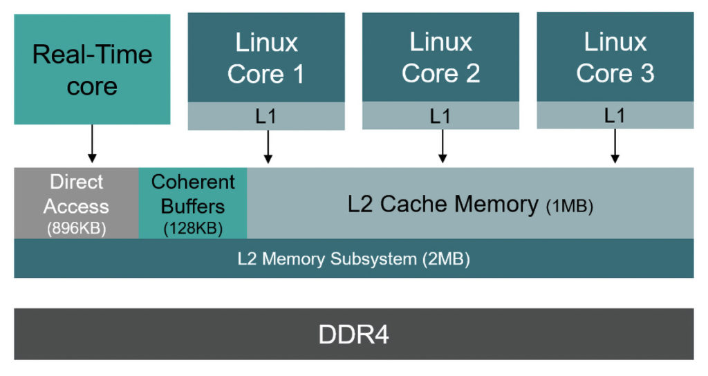
By contrast, the AMP implementation allows the developer to carve out a part of the cache memory, and reserve it for use exclusively by a real-time application. The PolarFire SoC supports both SMP and AMP modes, providing the developer with the freedom to choose one or the other, and even to change modes during field updates.
Once the AMP mode is configured in the PolarFire SoC, the real-time application can run on one of the application cores, a real-time core in which branch prediction has been turned off, as shown in Figure 3.
This hardware structure supports the fully deterministic operation of real-time functions alongside the Linux OS. In addition, interrupt service routing (ISR) execution times are deterministic, a claim which cannot be made as confidently for an SMP architecture implemented on an equivalent quad-core microprocessor based on Arm Cortex-A technology.

Fig. 3: In the PolarFire SoC AMP architecture, real-time functions access a dedicated portion of the L2 cache memory directly. (Image credit: Microchip)
Mastering hybrid FPGA/MPU system design
A hybrid FPGA/MPU SoC offers a unique ability to meet the requirements of certain kinds of application with a single chip. An application which concurrently performs local inferencing based on a machine learning model, and controls in real time the operation of a safety-critical motor, for instance, can implement the AI functions in the PolarFire SoC’s FPGA and the safety-critical controls on the multi-core processor.
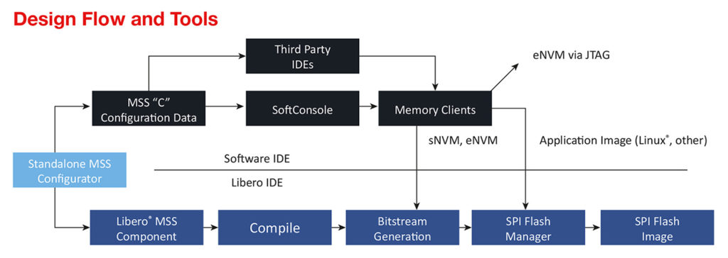
The presence of both an FPGA and an MPU on the same chip, however, means that the system design team has to work in two independent design environments. Both the PolarFire SoC’s toolchains feed into a configurator which generates:
The interaction between the two IDEs is shown in Figure 4.

Fig. 4: The relationship between the Libero IDE for the FPGA and the SoftConsole IDE for the MPU. (Image credit: Microchip)
Design simulation is also supported by separate tools: Renode for the software running on the multi-core processor part, and ModelSim for the FPGA part of the SoC. Microchip has also made good provision for debugging the complex applications which will run on the PolarFire SoC. Its on-chip-debugging mechanism communicates through a JTAG interface to debug tools:
Interestingly, the conditions for porting an application to the RISC-V environment are similar to those applying within the Arm environment. No two Arm core-based devices will have the same memory map, and equally no two RISC-V-based systems will share the same memory map. So porting from one Arm core to another requires in principle the same effort as porting from an Arm core to a RISC-V core.
A design-friendly operating and development environment
The PolarFire SoC, then, offers the advantage of integrating in a single chip both programmable hardware capabilities and a high-performance, multi-core platform for software applications. This hybrid architecture does entail the use of two development environments in parallel, but Microchip has taken great care to provide the user with a comprehensive set of tools which are extremely well integrated, and provide the capability for design teams to work productively in:
Full technical and sales support for OEMs developing applications on the Microchip PolarFire SoC FPGA is available from Future Electronics’ field applications engineers and embedded specialists globally.
Share This

Get access to the latest product information, technical analysis, design notes and more
Be at the forefront of New Technology Innovations
Be at the forefront of New Technology Innovations
© 2024 Future Electronics. All rights reserved. Privacy | Terms & Conditions of Sale | Terms of Use | Accessibility