FTM / Security & Encryption / Future Electronics — How the MinE-CAP Controller Shrinks Bulk Capacitor Size


By Christophe Basso
Business Development Manager, Future Electronics
The market’s response to growing demand for lighter and more compact travel power adapters has been greatly enhanced by the advent of GaN power switch technology: the fast-switching capability of GaN high electron-mobility transistors enables the development of very high-density converters.
If the increase in switching frequency has led to a substantial reduction in the volume of the main transformer, however, one component remains difficult to shrink: the bulk capacitor. Together with the front-end bridge rectifier, this element performs true ac-to-dc conversion before feeding the downstream dc-dc converter with a rectified rail. Selection of the bulk capacitor is dictated by its voltage and current ratings: the highest voltage input determines the choice, and this often leads the designers to specify an oversized component which is difficult to accommodate in the enclosure.
Now Power Integrations has introduced a component which elegantly builds the required capacitance on the fly depending on the input levels. As this article shows, this produces a large reduction in the total system volume, helping designers to make further progress in increasing the power density of devices such as power adapters.
Determining the capacitor value
Before discussing the selection criteria for the bulk capacitor, let us look at the simplified front-end section shown in Figure 1. A bridge rectifier receives a sinusoidal voltage from a wall outlet and a capacitor performs the smoothing function. The output feeds a constant-power load which mimics a closed loop-operated converter absorbing a regulated power output.

Fig. 1: Simplified front-end bridge rectifier circuit
In Figure 1, the capacitor is charged when the input sinusoid exceeds the voltage across its terminals by two diode drops. The charge lasts roughly until the peak of the input line is passed. For the remaining time, the capacitor no longer acts as a receptor and becomes a generator feeding the load on its own until the next recharging event. The rectified voltage is thus made of peaks and valleys during which the converter loop adjusts the operating point to deliver a clean, ripple-free, output voltage.
The converter must be capable of operating at full load down to the valley point, and supporting the thermal stress at an average current value between the peak and the valley at the lowest ac input voltage. It is important to understand this point as it conditions the capacitor selection. Reducing its value might sound appealing to designers for size and cost reasons, but having too low a valley voltage will force the over-dimensioning of the converter at such a low input.
Consequently, overpower conditions are likely to apply at high line, putting the circuit’s compliance with safety requirements at risk. On top of this, hold-up requirements may also need consideration and affect the final selection.
Identifying capacitor constraints
Various electrical or physical parameters can affect the selection of a capacitor, but those of the highest importance are voltage and operating temperature; the latter is tightly linked with the rms current value. As the temperature rises and approaches the maximum specified in the datasheet, a derating factor must be taken into account to maximize operating lifetime. It is also common to see derating factors approaching 30% of the maximum voltage for aluminum electrolytic types, with a recommendation to increase this safety margin further as the part heats up.
In travel adapters operated at the lowest input, 85 Vrms, the rectified voltage peaks at 120 V and can increase up to 180 V in a system operating on North American mains at 127 Vrms. In a European outlet the mains can be as high as 265 Vrms, the maximum of the nominal 230 Vrms specification, and this biases the bulk capacitor at 375 V. Based on these figures, designers traditionally chose their bulk capacitor according to the highest input voltage: capacitors with a 400 V rating are very popular. Considering a nominal high-line operating voltage of 325 V (230 Vrms nominal), it provides a derating factor of 19% for the capacitor in normal operating conditions.
Capacitor temperature is affected by the rms current flowing in the component and the ambient temperature in which it operates. The rms current must be assessed in the worst-case condition and should guide capacitor selection. Ignoring this important stage can severely shorten the operating lifetime, and even cause component failure.
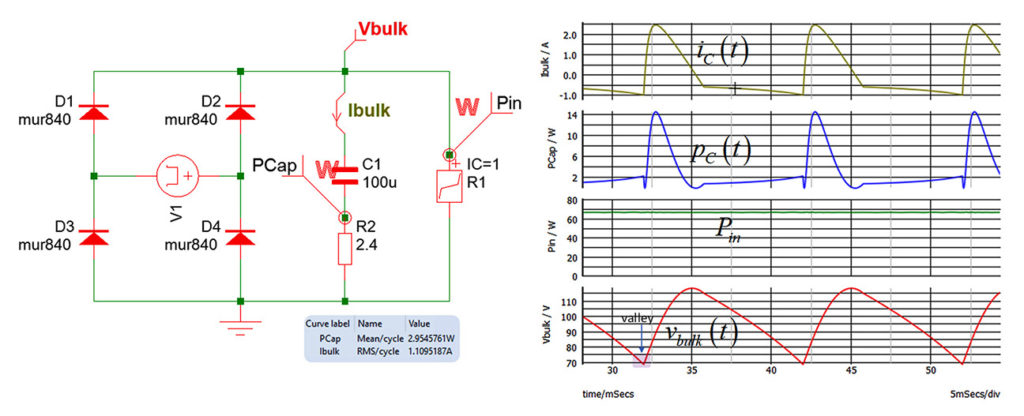
It is possible either to analytically compute the current1 or to rely on simulation to assess the rms content of the current circulating in the capacitor. Figure 2 shows a typical example with a SIMPLIS® circuit delivering the results in a few seconds. Here a capacitor with 2.4 Ω ESR produces a typical dissipation factor (tan) of 0.2 at 20°C temperature and a 120 Hz ripple current. The load is a 60 W adapter in this example.

Fig. 2: The front-end section consists of a diode bridge and a capacitor to perform ac-to-dc rectification
With a 33% voltage ripple, the valley voltage reaches 70 V: this value determines the size of the 60 W converter with a margin. Past the inrush surge, the rms current for the capacitor stabilizes around 1.1 A. In this simple set-up, the current is made of 100 Hz or 120 Hz cycles, but does not include the high-frequency pulses representative of the downstream converter signature. These pulses will also heat up the capacitor and must be accounted for in the evaluation process.
Selecting the right capacitor
The maximum allowable rms current varies substantially depending on the operating temperature. As is the case with many power components, the capacitor can carry more current when operating below its maximum temperature. Table 1 shows that, for a capacitor rated for a maximum temperature of 85°C, the maximum allowable rms current can be increased by 50% when operating at 55°C.

Table 1: Capacitor multipliers for the rated ripple current in relation to frequency and operating temperature
A similar case applies to the ripple frequency, where the worst case corresponds to the lowest frequency: the high-frequency pulses absorbed by a converter should have a lesser impact than the 100 Hz or 120 Hz ripple. In a 60 W adapter with the maximum temperature of the capacitor limited to 55°C, a 100 µF type accepting a current of 730 mA at 85 °C will be adequate.

Table 2: Operating the capacitor at a temperature lower than its maximum rating allows it to carry higher current
As confirmed by Table 2, any of the three highlighted components are potential candidates; the middle one provides some extra margin. This capacitor occupies a volume of approximately 12.7 cm3. A thermistor to limit the inrush current when the converter is plugged in will further increase the system’s board footprint.
In the simulation in Figure 2, when increasing the source to 230 Vrms the capacitor current drops to 585 mA, now making a 100 µF capacitor oversized. Also, if there is 30% voltage ripple, the effective capacitance could be reduced to a lower value of 68 µF or even 47 µF.
Capacitor tables will show that a more compact device could be used if the adapter were exclusively operated in high-line conditions. A large capacitor is required to accept the large rms current at low line, but also needs to be sized for 400 V operation when the rms constraint is less important. This raises the question of whether the capacitor value can be changed in response to changes in the mains input.
Capacitance on demand
This is the idea behind the Power Integrations MinE-CAP® controller: it enables the selection of a slim 400 V capacitor with a low rms capability for high-line operation, and in parallel a larger but 160 V-rated capacitor when the adapter operates at low line. Figure 3 depicts the principle in which two capacitors are mounted on the board.

Fig. 3: The controller from Power Integrations ensures the right capacitance is selected depending on the input voltage
At the first power-on sequence, the high-voltage capacitor CHL is immediately charged but limits the in-rush current owing to its low value. The controller then senses the input level and understands whether it is in high- or low-line operation. If it is high line, then a signal is sent to the downstream power supply controller, which immediately starts switching because operating conditions are met with CHL in place. At the same time, the controller starts slowly charging CLL with a constant-current source and thus avoids any associated current surge.
The charge sequence ends when the voltage across this capacitor reaches 145 V typically. The voltage across the capacitor is then regulated by the controller. When the adapter’s input voltage drops to a lower value, the controller waits until the voltage across the main capacitor CHL matches that of CLL before engaging the paralleling process. This is to avoid any current spike when associating capacitors which feature different voltage levels across their terminals.
Should the input voltage go up again and pass a predetermined threshold, then the low-line capacitor CLL would be safely disengaged and returned to trickle-charge mode. The process changes if the first power-on sequence occurs at low line. In this case, the low-line capacitor would be charged at a faster current, and once all voltages are within the expected window, the downstream switching converter can start operations. The datasheet typically mentions a start-up time of 250 ms from the initial ac connection in this mode.
If the high-line capacitor connects directly to the bridge rectifier, capacitor CLL goes through the internal MinE-CAP switch. This transistor’s performance is affected by a typical on-resistance of 620 mΩ at the highest operating junction temperature of 100°C. It is therefore important to verify that the rms current contributed by the low-voltage capacitor is consistent with the maximum power the package can dissipate while keeping the junction temperature in a safe area. Evaluating the junction-to-ambient thermal resistance, taking into account the PCB layout and copper thickness, is thus an important part of the design process.
A design example
This design process can be illustrated with an example, showing the calculation of front-end capacitance for a 65 W adapter running from a universal mains input down to 85 Vrms. Assuming 42% ripple and an acceptable valley voltage down to 70 V, the capacitance is calculated as 112 µF, normalized to the upper value of 120 µF. The simulation from Figure 4 reveals a ripple current of 1.3 Arms. In the Nichicon portfolio of 400 V aluminum capacitors, three parts from the UCY series would be suitable when operated below the maximum temperature of 105°C.

Fig. 4: According to simulation and data-sheets, three capacitors from Nichicon could be potential candidates
The volume of these capacitors is between 8cm3 and 9cm3, and could support the entire input-voltage span alone. Beside Nichicon, Surge Components also offers a rich selection of capacitors for these rectifying functions: parts in the RLA or RLD series would also fit the bill.
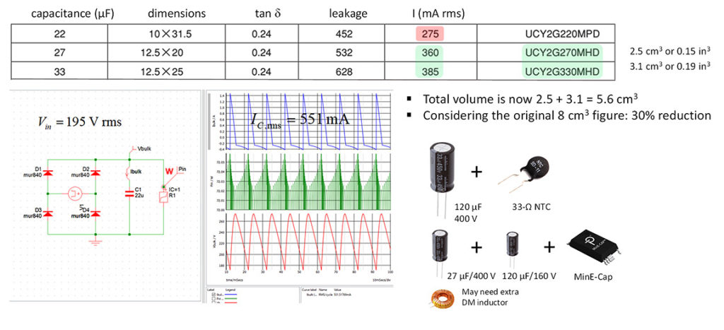
Narrowing down the search to 160 V types only, a 150 µF capacitor type would be suitable. It is described in Figure 5.

Fig. 5: The 160 V capacitor shows a significant volume reduction compared to the high-voltage type
The low-voltage type offers a valuable volume reduction of 51% compared to the high-voltage version initially selected. Running the same simulation at a 195 Vrms input, which corresponds to the low level of the 230 V nominal voltage, the rms current is calculated at 551 mA. A 22 µF capacitor will make the valley voltage go down to around 180 V: this is acceptable for the downstream converter. A look at the datasheets for this high-voltage part shows that a 27 µF or 33 µF capacitor would be suitable for this role.
Figure 6 shows the comparison of a circuit with a single high-voltage part and another with two capacitors covering the different voltage ranges: the total volume reduction provided by the dual-capacitor solution amounts to 30%, a substantial saving for a designer of high-density power adapters. And of course, a 160 V capacitor costs less than a 400 V type.

Fig. 6: Teaming two capacitors of different voltage and capacitance in lieu of one large capacitor is advantageous for volume and cost reasons
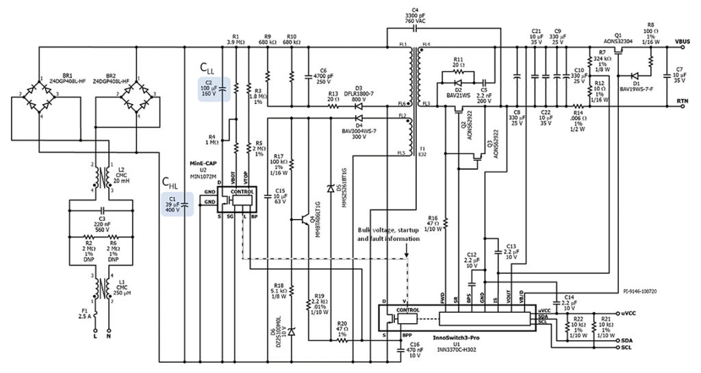
The MinE-CAP controller is designed to team up with a Power Integrations switcher such as the InnoSwitch™3-PRO described in the application report DER-626. The electrical diagram is reproduced in Figure 7. In this high-density 65 W adapter, the MinE-CAP pairs a 39 µF/400 V capacitor with a lower voltage 100 µF/160 V device.

Fig. 7: The application schematic shows the MinE-CAP® controller in the front-end section of the converter
The MinE-CAP and InnoSwitch devices share a common Vcc rail, the level of which is set by a Zener diode-based regulator. An auxiliary winding delivers the raw dc voltage and offers the best stand-by performance. When operating conditions are valid, the MinE-CAP controller enables the adapter by biasing the brown-out pin of the InnoSwitch circuit, and the adapter can supply one of four possible output voltages between 5 V and 20 V.
Conclusion
If the operating frequency increase in a switching converter helps to reduce the size of magnetic components, it plays no role in decreasing the bulk capacitor volume. In space-constrained designs such as high-density adapters, the selected capacitor can cause design problems because of the large size of components rated for as much as 400 V.
By combining two capacitors of different voltages, the MinE-CAP controller offers a clever solution to reduce the volume occupied by the front-end section. Designed as a companion chip to drive a downstream converter such as an InnoSwitch device, the combination offers a useful solution for designers of valuable high-density adapters.
More information about the Power Integrations MinE-CAP product may be found at: www.power.com/products/mine-cap/mine-cap.
Reference
Share This

Get access to the latest product information, technical analysis, design notes and more
Be at the forefront of New Technology Innovations
Be at the forefront of New Technology Innovations
© 2025 Future Electronics. All rights reserved. Privacy | Terms & Conditions of Sale | Terms of Use | Accessibility