FTM / Intelligent Lighting / Future Electronics — GaNSTar Demonstration Board
By David Woodcock
Centre of Excellence Manager, Future Electronics
Read this to find out about:
In the dc-dc converter stage of a high-voltage power supply for loads of more than around 150 W, the preferred choice of topology is the resonant LLC, because of its high efficiency. Nearly all existing LLC dc-dc converters are implemented with silicon power switches, but the replacement with gallium nitride (GaN) power switches on the primary side promises substantial savings in size and weight while maintaining high efficiency.
The switching frequency of silicon MOSFETs in conventional LLC dc-dc stages hits a practical ceiling at around 100 kHz, as switching losses become excessive at higher frequencies. GaN switches on the other hand can comfortably switch at frequencies of higher than 250 kHz, maintaining high efficiency and enabling the use of smaller and lighter magnetics and an overall increase in power density.
The practical implications of designing a 500 W LLC dc-dc converter using GaN switches have, however, not been well documented. Now, the Centre of Excellence (CoE) at Future Electronics has developed GaNSTar, a GaN switch-based design for a 500 W LLC dc-dc power stage which steps a 400 V dc input down to a 48 V output. In designing the board, the CoE explored the key issues that arise when using fast-switching GaN components in a high-voltage LLC dc-dc stage.
The characteristics of GaN power switches such as the STMicroelectronics MasterGaN1 integrated driver+switches used in the GaNSTar design are well understood. The CoE design team’s work, however, revealed interesting facets of the transformer operation. As is described below, the temperature of the transformer turned out to be the main constraint on the operation of the board.
The GaNSTar project was also able to develop an approach to implementing digital control as an alternative to the growing selection of off-the-shelf high-frequency LLC controllers coming on to the market.
Achieving conversion efficiency of 96% and using no more than a small fan for cooling at a load of 500 W, the GaNSTar board shows that a GaN switch-based LLC converter can be some 30% smaller than an equivalent design using silicon MOSFETs.
Key components: what is best, and what is available?
The GaNSTar board implements the familiar resonant LLC topology, shown in Figures 1 and 2. On the primary side, the half-bridge is implemented conveniently with a single component, the 600 V MasterGaN1. For most power-system designers, a device such as MasterGaN1 that integrates optimized gate drivers for the GaN power switches in a single package is preferable to a solution with discrete switches and drivers. This is because GaN switches are more difficult to drive than silicon MOSFETs. When driving GaN switches, circuit parasitics should be minimized. In addition, the gate can be damaged if the gate-source voltage exceeds 8 V, in most cases. With its MasterGaN family, ST provides a ready-made way to implement GaN in a design while also enabling a reduced component count and board footprint.

Fig. 1: The block diagram of GaNSTar shows how digital control is implemented on the primary side
On the secondary side, GaNSTar implements a full-bridge with four 100 V silicon MOSFETs, also from STMicroelectronics. The secondary side could have been configured in a half-bridge, but this would have required the use of MOSFETs that had a higher voltage rating of at least 150 V to support an output voltage of 48 V. The full-bridge configuration allows the use of 100 V MOSFETs: these are cheaper and more readily available than MOSFETs that have a higher voltage rating.
Using 100 V MOSFETs also leaves open the option to replace the silicon MOSFETs with 100 V GaN power switches as market availability widens, to gain extra efficiency. On this point, the gate driver selected on the secondary side of GaNSTar, the STDRIVEG600 from STMicroelectronics, is compatible with both silicon MOSFETs and GaN FETs.

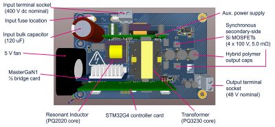
Fig. 2: The layout of the GaNSTar board
The key architectural decision in the development of GaNSTar concerned control: digital and programmable using a microcontroller, or analog control via an off-the-shelf LLC controller?
Various factors influence the choice for the designer. A programmable digital power system offers the flexibility to support multiple design iterations, which can be useful when developing a family of power supplies. On the other hand, an off-the-shelf LLC converter eliminates the need for software development and reduces development time and effort.
Until very recently, the market had not met the emerging need for LLC converter controllers for power supplies operating at frequencies above 100 kHz at full load. In 2022, this situation started to change: most notably, NXP Semiconductors released the TEA2017. This is a combined PFC controller and resonant LLC controller that supports switching frequencies well above 250 kHz in the LLC dc-dc stage, and that operates in continuous conduction mode (CCM) as well as in boundary conduction (BCM) or discontinuous conduction mode (DCM) for the PFC operation.
Other attractive options include the NCP13994 LLC controller from onsemi. For an ac-dc power supply, the NCP13994 could be paired with the NCP1680 totem-pole PFC controller.
Like NXP, STMicroelectronics offers a combined PFC and LLC controller, the STCMB1. The PFC controller supports BCM and DCM, however, but not CCM, so it is only suitable for loads up to around 250 W.
Rather than these off-the-shelf options, the GaNSTar design team opted for a flexible digital control option using an MCU from the STMicroelectronics STM32G4x4 Hi-resolution line, which is particularly suitable because of its provision of a high-resolution timer, complex waveform builder and event handler for digital power conversion.
The STM32G4x4 Hi-resolution line MCUs have capabilities that exceed the requirements for LLC stage control alone. Its location on the primary side of GaNSTar allows scope for further development in the future to incorporate PFC stage operation.
To achieve digital LLC control on the primary side using the STM32G4x4 requires a method for transferring the LLC converter’s output-voltage feedback signal across the isolation barrier. The GaNSTar design offers two options. The first uses a linear isolation amplifier that has a relatively high cost. This circuit achieves stable and efficient operation.
Two digital control loops have been implemented using this feedback path. Proportional integral derivative (PID) control offers an adequate response time. The CoE has also implemented a more advanced filtered PID control scheme which improves response time substantially, cutting the typical time to respond to a 20% to 80% change in load from around 500 µs with basic PID control, to around 300 µs.
The second option uses a standard combination of a TL431 shunt regulator and an optocoupler in a novel approach. Using an optocoupler potentially limits control-loop response time, since it has relatively low bandwidth. Applying a cascode-connected PNP bipolar transistor to the photo-transistor in the optocoupler increases bandwidth. An optocoupler bandwidth of 45 kHz is achieved by this approach.
The control loop operation is split: part analog and part digital. The TL431 is configured as an integrator providing high gain at low frequency. The STM32G4x4 performs digital processing of the error signal from the optocoupler to produce control-loop operation very similar to the filtered PID approach, but at a lower BoM cost than the first approach based on an isolation amplifier.
A schematic of the GaNSTar circuit is shown in Figure 3.

Fig. 3: GaNSTar circuit schematic showing the half-bridge on the primary side and full-bridge on the secondary side
Thermal limitation at the transformer
Laboratory testing of a prototype of GaNSTar revealed where the main design constraint lay, and it was not in the fast-switching GaN components.
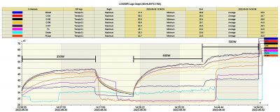
Under convection cooling, operation is limited to 300 W, due not to the temperature of the power switches, but of the transformer. The results gained under convection cooling are shown in Figure 4. At a power output of around 350 W with convection cooling and an ambient temperature of 25°C, the transformer’s temperature is higher than 90°C. This is uncomfortably high given that many applications for a high-voltage GaN-based LLC converter will actually run in ambient temperatures above 50°C. This thermal performance is a result of the transformer’s combined core and copper losses at high switching frequency and high current.

Fig. 4: Component temperatures when convection cooled at ambient laboratory temperature and increasing load
At ambient laboratory temperature, at the rated 500 W output, the MasterGaN1 operates at a temperature of just 42°C when cooled by a simple 5 V fan providing 7 CFM of airflow. This performance does not require elaborate thermal management, in GaNSTar, the MasterGaN1 has nothing more than a small, low-cost ceramic heat-sink.
As Figure 5 shows, when fan-cooled, all components operate at relatively low temperatures; the secondary-side silicon MOSFETs are the hottest components, reaching a temperature of around 65°C at 500 W load.

Fig. 5: Thermal plot of the GaNSTar components under fan cooling
The GaNSTar design, then, demonstrates that the practical limit of the power output from a GaN-based LLC converter is likely to be set by the temperature of the transformer. This design shows that an LLC converter can reliably supply a 500 W load with a small amount of forced-air cooling and minimal heat-sinking. Many options remain to increase the power output, including the use of a more powerful fan, and applying a heat-sink to the transformer core. Applying planar magnetic design techniques may also improve performance.
Other lessons learned during the development of the board
The most important finding to emerge from the development of the GaNSTar board is that GaN technology produces substantial space savings. At 66 mm x 116 mm x 40 mm and switching at 250 kHz, the GaNSTar board is around 30% smaller than an equivalent 500 W LLC converter based on the use of silicon MOSFETs switching at up to 100 kHz. Designers of production systems can expect even greater space savings, as they can adopt design optimizations that were not appropriate for GaNSTar, which is a demonstration design board.
Beyond this, the CoE engineers made additional findings that power-system designers should consider when building new systems based on GaN power switches:
For advice on these or any other technical issues involved in implementing a GaN-based LLC converter, designers should contact the power experts at the Future Electronics CoE to benefit from their practical experience with GaN technology.
Sign up for access to exclusive development boards, an essential tool for many innovative design projects.
*Available to pre-qualified EMEA customers only.
Be at the forefront of New Technology Innovations
Be at the forefront of New Technology Innovations
© 2024 Future Electronics. All rights reserved. Privacy | Terms & Conditions of Sale | Terms of Use | Accessibility